Pressmeddelande —
Areas where UV laser cutting systems are used, LPKF laser & Electronics AG
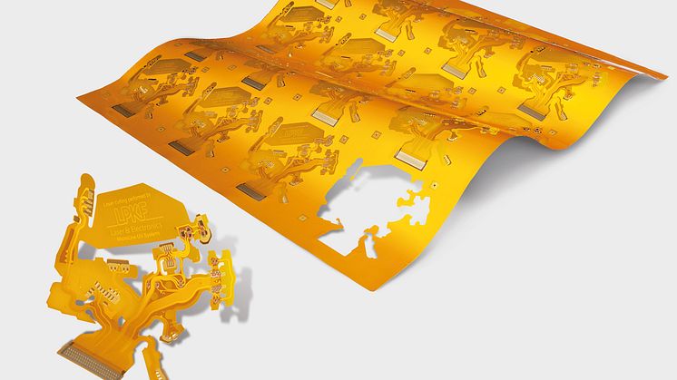
UV laser cutting systems show their special strengths with small,
thin and flexible circuit carriers. Depending on the thickness of
the circuit board material, one or several cuts along the desired
contour are required. The thinner the material, the quicker the
cutting process goes. If fewer laser impulses are emitted than
are required for penetrating the material, engraving of the
substrate takes place. In this way, clear component markings
for tracking & tracing can be applied during the separation
process.
Flat materials can be easily held in position by a vacuum table,
since the cutting process has no mechanical effects on the
material to be cut. For protection of strip conductors, cover layers
are applied to flexible interconnect devices. They often consist of
polyimide and glue with a thickness of 25 µm or 12.5 µm and are
sensitive to deformations. Individual areas – e.g., soldering pads
– have to be separated from the cover layers. This processing is
also one of the strengths of UV lasers.
For cutting entire contours, LPKF recommends a maximum thickness
of 0.8 millimeter; for webs, up to 1.0 millimeter. By means of multiple
cutting, noticeably larger material thicknesses are also possible –
with sensitive and valuable circuit boards, the longer cutting times
recede into the background compared to the safety and quality
aspects.
That also applies to decap applications and pockets in multilayers:
the UV laser cuts rigid and flexible components or extracts areas
from multilayer circuit boards so that components can be embedded
flush with one another. Technically this is no problem if the area of
the pockets is not laminated. The penetration depth of the UV laser
can be controlled so precisely that layers underneath are not
damaged.
Läs mer...
Contactperson in Sweden: Mr. Gerhard Tetzlaff
Phone: +46-40-536614, E-mail: gerhard.tetzlaff@solectro.se
--------------------------------------------------------------------------------------------
Ämnen
Kategorier
Regioner
Solectro AB grundades 1983 av Gerhard Tetzlaff.
Verksamheten omfattas av utveckling, produktion, försäljning och service av komponenter för automatisering, komplettlösningar, specialmaskiner, robotar, CNC-maskiner,PCB-prototying, laser, SMD samt dentalmaskiner.
Solectro AB är beläget i Lomma - ca. 10 minuter från Malmö och Lund.
Adress:
Tenngatan 6 - 8, 234 35 LOMMA
Tel. 040-536600
Fax 040-536610
E-mail: solectro@solectro.se
www.solectro.se