Image -
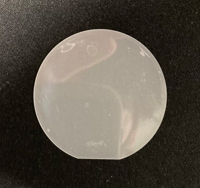
NGK_Next-generation power semiconductor water prototype (2-inch wafer).jpg
go to media item
- License:
- Media Use
The content may be downloaded by journalists, bloggers, columnists, creators of public opinion, etc. It can be used and shared in different media channels to convey, narrate, and comment on your press releases, posts, or information, provided that the content is unmodified. The author or creator shall be attributed to the extent and in the manner required by good practice (this means, for example, that photographers should be attributed).
- File format:
- .jpg
- Size:
- 636 x 599, 109 KB