Pressmeddelande -
PCB Processing with UV laser systems, LPKF Laser & Electronics AG
More complicated circuits and increasing space problems demand new
solutions in processing printed circuit boards. Many products require
irregularly shaped contours, combinations of rigid and flexible materials,
webs in the immediate vicinity of sensitive components and strip
conductors as well as adaptability to product changes. Cutting with
UV laser systems offers a clean and economical solution.
Admittedly, with simple circuit board layouts, conventional processes are
one step ahead in separating individual circuit boards from larger boards.
Saws can very quickly detach rectangular boards from a larger carrier if
neither the mechanical load nor the formation of dust are critical. Punching
machines are the first choice when producing large numbers of pieces without
layout changes.
The alternative to this is contour milling. Usually contours are milled out before
assembly except for narrow webs. The mechanical loads when milling contours
and when manually breaking webs loose are often a criterion for exclusion.
Sensitive boards suffer due to vibrations, breaking loose is imprecise and the
throughput is low and has high testing costs.
Laser cutting systems
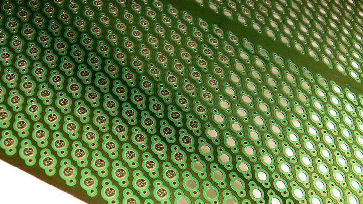
Fine, compactly assembled electronic circuits are especially sensitive to
mechanical stress, dust and geometric deviations. Laser cutting systems
present themselves here as the better alternative. They prevent mechanical
loads, reduce tool costs, are more precise and facilitate larger net usable
surfaces. Another challenge in electronics production is the constant increase
in variability. Short-term orders, frequent layout changes and small lot sizes
require flexible production processes. Here, too, laser cutting systems present
themselves as the better alternative.
With sensitive substrates, irregular contours, narrow cut channels and frequent
layout changes, laser cutting systems can be impressive. But here, too, clear
differentiations are meaningful, because lasers of different wavelengths also
interact differently with the material.
For example, CO2 laser systems are used with a wavelength of ca. 10.6 µm
(far infrared). They are comparatively inexpensive to produce and are available
in high output classes up to several kW, but also bring a lot of heat into the cut
edge and cause a noticeable carbonation of the organic circuit board
components at the margins. CO2 lasers cannot be easily guided in optic fibers,
but instead have to be brought to their destination via open mirror systems.
They are primarily used with thicker circuit boards.
If things have to become noticeably finer, it is time for UV laser systems.
As Nd:YAG systems, UV lasers have a wavelength of 355 nm through
frequency tripling – this radiation can be focused well through the use
of optics. UV lasers are suitable for cutting and marking thin rigid, flex-rigid
and flexible PCB substrates and auxiliary foils. Outputs of around 10 watts
are concentrated on a focus diameter of only 20 µm; the results obtained
are accordingly exact. The energy acts on the material for only fractions
of a second without thermal impairment of the component. The cutting
gases that arise are exhausted and filtered. Strip conductors close to the
edge and soldering points remain intact due to the minimal cut widths; no
burrs arise.
In addition, the cost for tools or elaborate holding fixtures and the corre-
sponding lead times for their production are dispensed with. With thin
substrates, a vacuum table is sufficient for ensuring a level substrate
position.
When laser cutting, a change of the cutting contour takes place via changing
the layout data. The machine software takes over the data formats from all
current layout programs. It relies on a stored library with cutting parameters
that have been proven in practice for cutting different materials.
Laser cutting does not create significant edges. The contactless process
requires almost no circuit board surface as a cutting channel; the components
move right up to the edge. Due to the laser cutting process, more components
can be placed on a single printed circuit board and at the same time more
panels can be accommodated on one board.
UV laser cutting is also used in processing thin flexboards because it can take
into account the frequently occurring deformation of the material after reflow
soldering. UV laser cutting systems from LPKF detect the deformation of the
soft material at several positions with an integrated vision system and provide
for standard- and tolerance-compliant final circuit boards with dynamic position
correction.
Read more...
Contactperson in Sweden: Mr. Gerhard Tetzlaff
Phone: +46-40-536614, E-mail: gerhard.tetzlaff@solectro.se
--------------------------------------------------------------------------------------------------------
Ämnen
Kategorier
Regioner
Solectro AB grundades 1983 av Gerhard Tetzlaff.
Verksamheten omfattas av utveckling, produktion, försäljning och service av komponenter för automatisering, komplettlösningar, specialmaskiner, robotar, CNC-maskiner,PCB-prototying, laser, SMD samt dentalmaskiner.
Solectro AB är beläget i Lomma - ca. 10 minuter från Malmö och Lund.
Adress:
Tenngatan 6 - 8, 234 35 LOMMA
Tel. 040-536600
Fax 040-536610
E-mail: solectro@solectro.se
www.solectro.se